Microchips
These tiny but mighty components power artificial intelligence (AI) systems, and they've been getting faster and more powerful. The development and fabrication of microchips is complex and expensive, and the use of cloud computing and other decentralized computing techniques can make it difficult to determine who owns the data used to train AI systems. This, along with microchip security concerns, adds deep complexity to the AI policy puzzle.
Updated September 2024
This section of the AI Policy Guide provides an overview of how microchips function and how they are manufactured and used. To craft effective rules, policymakers must have a firm grasp of each of these aspects.
In 1997, the addition of a tailormade “chess chip” allowed IBM’s Deep Blue artificial intelligence (AI) system to defeat world champion Gary Kasparov in chess. This defining moment in AI history was enabled by improvements in the engineering of semiconductors and the manufacture of microchips (or simply, chips). Since then, a recurring theme in AI innovation has been the importance of ever more efficient chips. Without the significant improvements in microchip capabilities since 1997, none of the big data or machine learning strategies that have supplanted the more primitive AI methods used by Deep Blue would have been possible.
Microchips serve two primary purposes in AI: providing processing power and storing data. Perhaps their most important quality, however, is the speed that enables quick computation and, by extension, intelligence. This section discusses how microchips function and addresses the increasing importance of this element to AI innovation.
Microchips have many important aspects:
AI systems depend on microchips to run AI algorithms and store data.
Variations in chip design can offer unique functions, speeds, and storage properties to AI systems.
Chips are increasingly AI specific. Popular AI-specific designs include graphics processing units and application-specific integrated circuits.
Over the past four decades, microchips have improved exceedingly quickly, doubling their processing speed roughly every two years by physically shrinking computational units. Owing to physical limits, however, this geometrical pace may not be sustainable over time. Future chip innovation will depend on architectural innovation.
Microchip design and manufacturing are complex and supported by a wide range of disciplines, technologies, and companies.
Microchip and AI Chip Basics
This section discusses microchip basics and AI chips.
Microchip Basics
Although separate concepts, microchips are often referred to as semiconductors. The name “semiconductor” comes from semiconductor materials, such as silicon or germanium, the key ingredient in chips. Chips contain many components, but their power and speed are owed to their transistors, the semiconductor switching device that performs computation. As a rule, chip power and speed increase as the transistors on a chip shrink in size and grow in density—that is, more transistors fitted into the same space. Historically, chip innovation has been linked to transistor innovation (specifically, transistor size reductions). For decades, consistent transistor improvements have unleashed the ever-growing processing speeds that, in the 1990s, enabled systems such as Deep Blue and, in the modern era, machine learning.
Chip innovation has long followed a pattern, known as Moore’s law, in which the number of transistors per chip doubles roughly every two years. Less a “law” and more an observation of chip innovation patterns, Moore’s law has nonetheless held true over recent decades. The resulting pace of chip improvement has allowed for predictable improvements in the design of AI systems. For algorithms, this improvement has enabled greater processing speeds and therefore quicker “AI thinking.” For data, this advancement has built the storage capacity needed to support big data. Transistors, however, are shrinking to their physical limits, and their performance no longer will advance as quickly, if at all, on the basis of size alone. Future improvements in chip function, and by extension AI, will require innovation beyond shrinking the transistors inside microchips.
The past stability in the rate of growth of processing power meant that AI research focused on algorithms, sidelining discussion of hardware. In recent years, however, hardware is at the center of the AI conversation. To meet processing demands, researchers are turning to AI chips (also called AI accelerators), a range of chips that are designed specifically for the unique processing needs of AI. AI chips improve performance not through transistor size reductions but via changes in microchip architecture—the “blueprint” configuration of chip components.
The AI chip advantage is rooted in speed and specialization. Central processing units (CPUs), the general-purpose chip used for AI before the emergence of AI chips, are flexible but less efficient than AI-dedicated chips when processing AI-specific calculations. CPUs perform inefficiently when operations are repeated in bulk and when memory is frequently accessed, which are requirements of most AI algorithms. AI chips can solve these problems.
In brief, in addition to CPUs, there are currently three categories of AI chips that policymakers should understand: graphics processing units (GPUs), field-programmable gate arrays (FPGAs), and application-specific integrated circuits (ASICs). GPUs, FPGAs, and ASICs can be conceived of as standing on a spectrum spanning greater flexibility at the GPU end and greater speed at the ASIC end, with FPGAs standing in the middle.
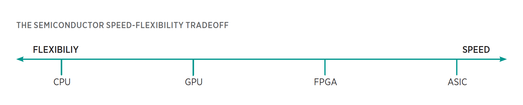
GPUs are limited-purpose chips originally designed for graphics processing, but they have been appropriated for AI. Training a neural network, the most common AI model, requires large-scale and frequent matrix multiplication, a simple yet time-consuming mathematical operation. GPU architecture is designed with many matrix multiplication units that can execute multiple operations simultaneously, a quality known as parallelism. To analogize, a CPU is like an expert chef—versatile at cooking any dish simple or complex, though limited in that he or she can cook only a handful of dishes a night. GPUs are like an army of fast-food cooks—their versatility is low, and the food is not complex, but through raw numbers and focusing on only a few menu items, these cooks are able to feed far more people each night.
FPGAs and ASICs are single-purpose chips custom built for each application. In both, the AI software is hard-coded directly into the chip’s silicon base. Application specificity increases speed by removing unneeded features and streamlining computation. The core difference between the two is programmability: the circuits baked into FPGAs are custom built and can be updated as needed. Meanwhile, ASICs are custom built but cannot be updated. FPGAs, owing to their programmability, carry certain efficiency costs. ASICs are perfectly tailored to an application’s specific needs, giving them greater speed.
Chip selection depends both on the phase of AI deployment and application-specific inference demands. GPUs, owing to their flexibility and parallelism, command the vast bulk of chips used to train systems. During inference, however, application-specific demands have led to greater diversity. For speed-critical applications, such as real-time monitoring systems, the superior speed of ASICs can be critical. For some consumer products, pricing is key, favoring CPUs over comparatively expensive AI chips. Overall, the growing trend in AI inference chips is a steady gain of market share by ASICs.
Often, floating point operations per second (FLOPS) are used to measure processing power and intensity. A floating point operation is any basic mathematical operation (addition, multiplication, etc.) on rational numbers (that is, numbers with decimal points; for instance, 3.12). Measuring the number of operations per second gauges how quickly processors run computations and programs. Confusingly, floating point operations—FLOPs, with a lowercase “s”—are also used to measure model “size” based on how many operations that model requires. Both are common in policy and computer science literature.
Microchips in Detail
This section discusses microchips in detail, along with chip design and manufacturing.
What makes silicon and the other semiconductor materials that power computing unique is their ability to act both as insulators and conductors, depending on certain conditions. This quality is significant because it allows engineers to program exactly when these materials will conduct electricity. The working part of chips made of semiconductor material is the transistor. Functionally, a transistor is an electronic switch that alternates from allowing current to flow to blocking current. When current flows, it is represented as a 1, and when it is blocked, it is represented as a 0. This core function forms the basis of data representation and computation.
Transistors are built from a combination of silicon and dopants, impurities that alter the properties of conductivity to enable engineers’ discrete control over electric currents. Without dopants, engineers could not control when and why a transistor switches on or off.
To manipulate and store electrical currents, one can link transistors together in circuits that enable them to perform basic computation. For instance, an adder is a common circuit that takes in two numbers and adds them together. Transistor circuits can also form memory units. For instance, static random-access memory (SRAM), a type of computer memory, uses a small collection of linked transistors to trap energy, thereby storing the data that energy represents.
Integrated circuits (ICs) are devices that string together many of these circuits, memory units, and other peripheral components to create a toolbox of basic operations that software engineers can use when running algorithms. ICs often include execution units, subsystems that package related circuits together with memory and other tools to enable basic functions. These execution units come in many forms, each with a specifically designed purpose. An arithmetic logic unit, for instance, may include an “adder” to perform addition, as well as all other circuits required for basic arithmetic. The toolset provided in a chip can vary widely, and supporting AI often means choosing chips with the ideal set of capabilities.
Chip Design and Manufacturing
Central to many policy questions are issues related to the design, manufacture, and supply chain of microchips. These systems are highly complex, and they are supported by a wide web of technologies and engineering disciplines. Ensuring AI innovation naturally involves ensuring a robust and secure supply chain.
Talent. The skills required to develop AI chips are fundamentally different from those needed for AI algorithms and data management. The scientists who design AI chips tend to be electrical engineers by trade; algorithms and data are the specialty of software engineers. Further, manufacturing requires an even more distinct skillset to develop the physical processes, machines, and production foundries. This requirement expands the necessary AI talent pool to include an array of disciplines, including chemical engineering, materials science, and mechanical engineering. AI innovation is not the domain of computer science alone.
Development and Application
Development and fabrication. Microchip development goes through several core phases. To design a chip, engineers wield electronic design automation (EDA) software that allows them to map a chip’s execution units and arrange transistors.
Once designed, chips are then fabricated in foundries where chips are not assembled but printed. In brief, the process starts with a wafer, a raw chip base, usually made of silicon. Next, a variety of materials are printed onto the chip to enable photolithography, a process by which light is shined through a “circuit stencil” known as a photomask, printing the design onto the chip. Additional elements are added through etching (using chemicals to remove unwanted material and shape the design) and deposition (blanketing the chip with materials to add components). The list of materials required spans a large portion of the periodic table. Therefore, manufacturing requires an extensive supply chain, materials stock, and a chemistry knowledge base to support manufacturing operations. After chips are printed, they are packaged in a protective casing and shipped.
Material science innovations are an often overlooked source of greater AI processing power. For instance, engineers have found that using thinner ultraviolet rays, rather than visible light, in photolithography can embed chips with thinner components, decreasing chip size and increasing chip speed. To reiterate, AI innovation is not the domain of only computer science.
As a generality, the equipment used in chip development and manufacturing is highly specialized and, as a result, highly expensive. Photolithography scanners, for instance, can cost more than $100 million per unit. Specialization has also led to concentration. In some cases, this concentration is geographical; for example, as of 2022, 85 percent of leading-edge chips were manufactured in Taiwan and the remaining 15 percent in South Korea. The Dutch firm ASML Holdings is the only manufacturer of the extreme UV lithography machines needed to make all state-of-the-art chips in use today. All of these factors complicate the robustness and security of the AI supply chain and have recently received significant policy scrutiny.
Hardware infrastructure. Once these chips are produced, their specific arrangement and use in AI systems are also essential to the power they unleash. Not all these hardware capabilities will be housed locally. Cloud computing, a general concept in which computing resources are stored remotely and can be accessed for a fee, helps provision resources. The cloud cheapens computational cost through economies of scale and lowers the barrier to entry for AI. This approach can allow researchers to access the resources they need without buying physical semiconductors. Naturally, this framework renders both the AI supply chain and the AI regulatory puzzle ever more complex. Pieces of an AI system can exist in multiple locations that collectively provide needed resources. Decentralized computing techniques such as federated learning further muddy the waters by eliminating centralized computing and data storage. This technique trains AI systems on a web of disconnected servers, rather than a centralized server, to eliminate data aggregation and preserve privacy. Such techniques could add regulatory complexity by eliminating the ownership link between AI engineers and the data they use.